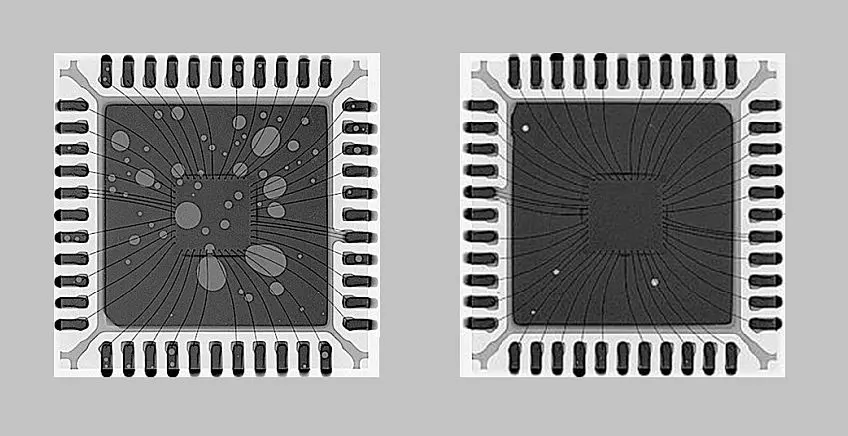
Nistec has exhibited a totally effective solution to the air bubbles (voids) phenomenon in solder joints by means of an innovative Vapor Phase technology.
News & Events
- July 31, 2025
The Nistec Company has announced that it has achieved a totally effective solution to a well-known and extremely critical problem in the soldering process of electronic components on PCB’s. The Production Plant succeeded in decreasing the air bubbles (voids) phenomenon in electronic components, particularly in components such as BGA and BTC, by means of an advanced Vapor Phase soldering system manufactured by the German company ReHM Thermal Systems.
The new system, CondensoXC VAC, enables a near-total diminution of air bubbles – voids – at a coverage level approaching 100% – owing to a unique combination of a vacuum process in the melting stage. During this operation, gases trapped within the solder joints are being pumped out, even before they solidify, thus avoiding the formation of thermal pockets that might harm the PCB´s functioning reliability as well as the mechanical strength between the electronic component and the PCB.
This technology enables an extremely high soldering reliability and it is intended for the provision of a precise and reliable response to the stringent requirements of the Company’s defense customers.
The IPC Class 3 Standard, which represents the highest level of quality and reliability for PCB´s, defines that the air pockets’ (voids) area at a solder joint may constitute up to 30% for BGA (Ball Grid Array) components and up to 50% for BT (Bottom Terminated) components (BTC). Nonetheless, customers who require extremely high solder reliability, such as defense customers, are interested in reducing the air pockets’ area, even beyond the Standard, as much as possible. Using this method, the air pockets’ area at a solder joint can be reduced at a rate of up to less than 1% of the overall soldering area.
The technology is based on a soldering method that utilizes vapors of a dedicated material called Galden (i.e. Vapor Phase Soldering), which enables a uniform and gentle heating of all the PCB’s components while incorporating vacuum activation at the melting point. The process is carried out within a closed chamber, into which the vapors are injected, and thanks to the physics of condensation, the heat is transferred accurately only up to the desired temperature – and thus, overheating, deformations and air bubbles (voids) beneath sensitive components are prevented.
The clear advantages for the customer are – minimal formation of bubbles below the components as well as high thermal reliability over time – this, thanks to the full connection between the component’s pad and the PCB’s pad.
“This is yet another step we have implemented in order to provide a technological response at the highest level to our customers”, said Arbel Nissan, the Company’s VP of Marketing and Sales. “In an era in which the components are becoming smaller, denser and more sensitive, our ability to deliver void-free soldering, provides an extremely advanced soldering capability”.
This move is integrated as part the strategic investment of Nistec in upgrading the production lines as well as providing an accurate response to the technological challenges of our defense and aeronautical customers in Israel and throughout the world.
More Articles
Nistec Newsletter #30 – Teardrops
Design Guidelines for Teardrops
Engineering PCBs for Production Excellence and Long-Term Reliability – Webinar February 2026
Engineering PCBs for Production Excellence and Read More