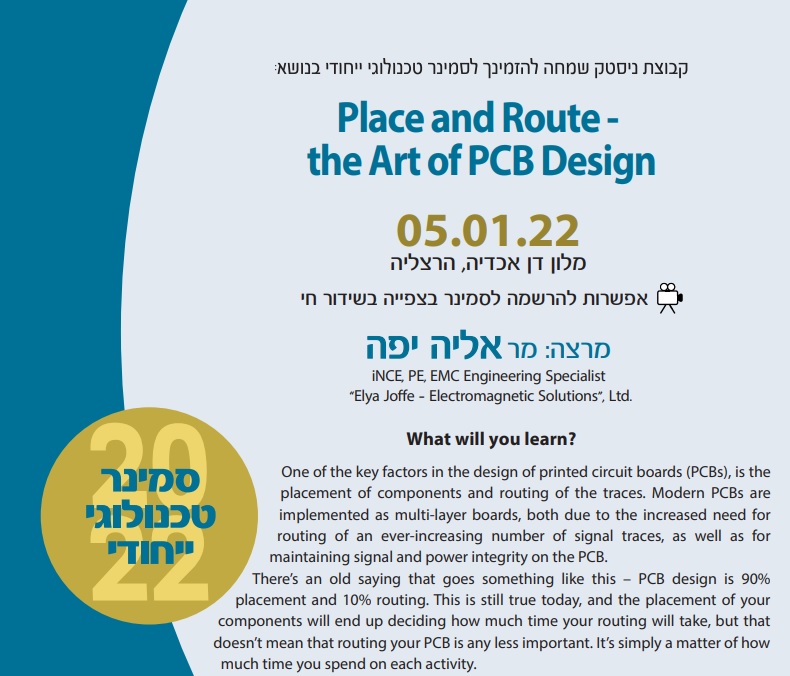
Technology Seminar – Place and Route – the Art of PCB Design – Elya B. Joffe – 05-01-22
Technology Seminar – Place and Route – the Art of PCB Design – Elya B. Joffe – 05-01-22. One of the key factors in the design of printed circuit boards (PCBs), particularly modern, high-speed PCBs, is the placement of components and routing of the traces. Modern high-speed PCBs are implemented as multi-layer boards, both due to the increased need for routing of an ever-increasing number of signal traces, as well as for maintaining signal and power integrity on the PCB. Here in this seminar, we will look at some best practices of PCB component placement and trace layout to help engineers create a superior design. It is truly an essential seminar. The unique technology seminar will be held at Dan Accadia Hotel, Herzliya (Live Broadcasting will be available too). Seminar agenda: http://www.nistec.com/wp-content/uploads/2021/11/Technology-Seminar-Place-and-Route-the-Art-of-PCB-Design-Elya-Joffe-05-01-22.pdf Registration now open: https://docs.google.com/forms/d/e/1FAIpQLSfjLdRbnOuCZqYJFgDRfEjdcjJ9W_G7cVGnhxhvCCeCNs1eBw/viewform

